Atum Works: The Startup Building the ASML of 3D Nanomanufacturing
Atum Works is a Mountain View-based startup on a mission to redefine the limits of semiconductor manufacturing through 3D nanolithography. Think of it as building the “3D version of ASML,” but instead of just stacking today’s tech on top of itself, they are architecting a completely new layer of reality—both literally and metaphorically—for how the next generation of chips and advanced materials are created.
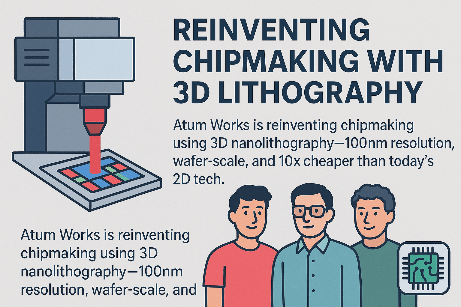
Founded in 2024 by a team of Caltech and NASA engineers, Atum Works emerged from stealth with a bold promise: to bring about the next scaling law in computing by fabricating multi-material 3D structures at 100 nm resolution across full wafers, all at a fraction of the cost of traditional 2D lithography. Their work sits at the convergence of nanotechnology, physics, and rocket-grade engineering—and it’s already attracting serious attention.
What Problem Is Atum Works Solving?
For decades, Moore’s Law reliably predicted the doubling of transistor density every two years, powered by 2D lithography techniques that continually shrank components on silicon chips. But the industry has now hit a wall.
As H.-S. Philip Wong, Chief Scientist at TSMC, put it in 2024:
“For the past 50 years, semiconductor-technology development has felt like walking inside a tunnel. The road ahead was clear. Now, we have reached the end of the tunnel."
The problem is simple yet monumental: 2D lithography can no longer keep pace with the increasing demand for density and performance. In response, manufacturers have started stacking layers—essentially going 3D with 2D tools—but this results in exponential cost increases. For instance, high-bandwidth memory stacks with 10 layers can cost five times as much as their unstacked equivalents.
That’s where Atum Works comes in—not to add layers, but to rethink the process entirely.
How Does Atum Works’ 3D Lithography Change the Game?
Atum Works isn’t just building better tools—they’re rewriting the rules. Their proprietary 3D lithography process creates nanostructures with sub-100nm precision using a completely different method of fabrication. Instead of layering 2D slices like a precarious lasagna, they build structures volumetrically with a level of resolution and complexity that opens the door to both miniaturization and function previously impossible in conventional semiconductor fabrication.
This approach brings a few powerful advantages:
- Scales with materials, not layers, avoiding the exponential cost curve.
- Multifunctional output, enabling not just advanced logic chips but breakthroughs in biotech, sensing, and advanced materials.
- Commercial viability: Having crossed key cost thresholds, their system is now practical to deploy at scale, and customers are already lining up.
By building in 3D from the start, Atum Works allows for new architectures, new physical configurations, and new applications across disciplines. And it’s not just theoretical—they’ve already built a working nano-printer and secured a letter of intent from NVIDIA.
Who Are the Founders Behind Atum Works?
Atum Works is led by three co-founders who blend bleeding-edge science with hands-on engineering grit:
- Lucas Pabarcius (CEO): A former physicist at Caltech and ex-NASA engineer, Lucas has worked on advanced optics and propulsion systems for missions like Starshade and Europa Clipper. Known for building the world’s fastest-burning hybrid rocket engine and for winning NASA’s “Most Visionary Concept” award, he now channels his vision into reshaping how matter is manufactured.
- Matteo Kimura: A computational mathematician who’s applied his skills to robots in space, between buildings, and near the Moon. His resume includes writing lunar flight software, directing space missions, and winning NASA contracts. Matteo brings an unmatched systems-thinking mindset to the company’s computational and control challenges.
- Malcolm Tisdale: An engineer who helped develop NASA’s Mars helicopter and designed multi-material manufacturing methods at Caltech. Malcolm’s prior leadership at Caltech Air and Outer Space and his award-winning dust-shielding technologies signal his deep expertise in material science and applied physics.
Together, they form a rare blend of precision, creativity, and execution—qualities essential to tackling a challenge this bold.
What Has Atum Works Accomplished So Far?
Though founded only in 2024, Atum Works has already reached several critical milestones:
- Established a manufacturing facility and laboratory in the heart of Silicon Valley, enabling rapid prototyping and iteration.
- Built its first functional 3D nano-printer, validating the core technology in real-world conditions.
- Acquired early customers, including a co-development partnership with NVIDIA, one of the world’s most advanced chipmakers.
- Proven commercial viability by crossing key cost thresholds that make their technology scalable and competitive.
Their rapid progress mirrors the trajectory of other legendary deep-tech companies, blending speed with scientific integrity.
What’s Next for Atum Works?
Looking forward, Atum Works has outlined an ambitious roadmap that includes:
- Product Sales: Shipping their first commercial products within the year.
- Scaling Manufacturing: Exponentially increasing production capacity to meet market demand.
- SECRET: As hinted in their launch materials, the team has more up its sleeve—perhaps entirely new applications or revolutionary techniques yet to be revealed.
With each step, the team aims to create a Moore’s Law-like feedback loop of exponential improvement, this time in three dimensions.
Why Does This Matter Beyond Chips?
While the immediate focus is on revolutionizing semiconductor manufacturing, Atum Works’ platform has the potential to impact a broad array of fields:
- Biotech: Creating nanoscale scaffolds for tissue engineering, drug delivery systems, or microfluidics.
- Sensors: Enabling compact, high-resolution sensing devices for everything from medical diagnostics to environmental monitoring.
- Advanced Materials: Developing new composite materials with previously impossible internal geometries or behaviors.
Where traditional fabrication hits walls, Atum Works opens doors to new physics, new devices, and new industries.
What Is the Vision Behind Atum Works?
Atum Works isn’t just a nanofabrication company—it’s a bet on the future of compute, matter, and possibility. The company envisions a world where gigascale nanomanufacturing is not just accessible, but foundational to progress in every domain of science and engineering.
Much like ASML became indispensable to the modern semiconductor industry by perfecting 2D lithography, Atum Works seeks to become the core enabler of 3D nanofabrication. Their aspiration isn’t incremental—it’s transformational.
Is Atum Works the Beginning of a New Scaling Law?
That’s exactly the goal. In a world where Moore’s Law has reached its twilight, Atum Works is ushering in a new sunrise—a scaling law not bound by layers, but by geometry, complexity, and material intelligence.
Their vision is radical. Their tech is working. And their timing is perfect.
If the last 50 years were about shrinking in 2D, the next 50 may be about building in 3D—and Atum Works plans to be the company that makes it possible.